The Invisible Sovereign: ASML and the Architecture of Modern Power
How a "leaky shed" in Eindhoven built a trillion-dollar moat and became the ultimate bottleneck for the AI era.

The World’s Most Critical Bottleneck
In the global race for silicon supremacy, all roads lead to a single, unassuming campus in Veldhoven, Netherlands. ASML is not just a semiconductor equipment manufacturer; it is the ultimate “toll booth” of the digital age. While the world obsesses over the AI chips designed by Nvidia or the fabs operated by TSMC, none of those titans can function without ASML’s Extreme Ultraviolet (EUV) lithography machines—the most complex pieces of machinery ever sold commercially. This is a company that transitioned from a leaky wooden shed in 1984 to a total global monopoly today, possessing a technological moat so wide that its only “competitors” are the laws of physics themselves. In this deep dive, we explore how ASML’s “bet-the-company” R&D culture, ironclad supplier lockdown, and high-margin service engine have created one of the most resilient compounding machines in industrial history.
🏗️Phase 1: The Leaky Shed (1984–1990)
In the early 1980s, the lithography market was dominated by Japanese giants Nikon and Canon. ASML was born out of a desperate attempt by Philips to offload a money-losing R&D project.
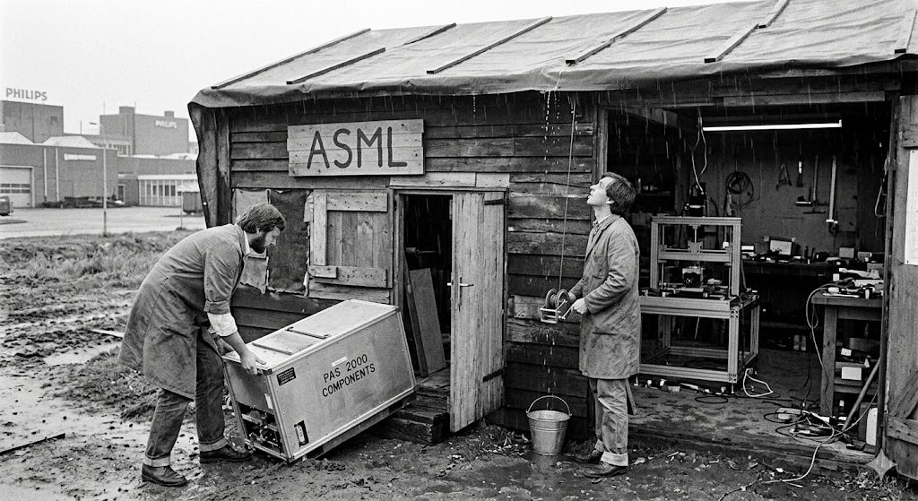
1984: The Founding. ASML is formed as a 50/50 joint venture between Philips and ASM International (ASMI). They start in a literal leaky wooden shed in Eindhoven, Netherlands.
1984: Launch of the PAS 2000, their first stepper. It fails to gain significant traction against Japanese competitors.
1986: A critical turning point. ASML signs a partnership with Carl Zeiss for lenses, a relationship that remains the backbone of the company today.
1988: ASMI (the partner) runs out of money and pulls out. Philips nearly shuts the project down but is persuaded by ASML executives to give it one last chance.
1988: ASML establishes a joint venture in Taiwan, giving them a foothold in the emerging Asian foundry market (early ties to what would become TSMC).
🚀 Phase 2: Independence & The DUV Breakthrough (1991–2000)
The 90s saw ASML transition from a “fast follower” to a legitimate threat as they mastered Deep Ultraviolet (DUV) light sources.
1991: Launch of the PAS 5500. This machine is the “Model T” of ASML—it is modular, incredibly productive, and brings in the cash flow needed for independence.
1995: IPO. ASML goes public on the Amsterdam and NASDAQ exchanges. Philips begins divesting its stake, and the capital injection allows ASML to scale R&D.
1997: ASML begins investigating Extreme Ultraviolet (EUV) light—a wavelength of 13.5 nm—long before it is considered commercially viable.
1999: ASML joins the EUV LLC, a US-led consortium (including Intel) to explore EUV research from US National Labs.
🌊 Phase 3: Market Dominance & The Immersion Era (2001–2010)
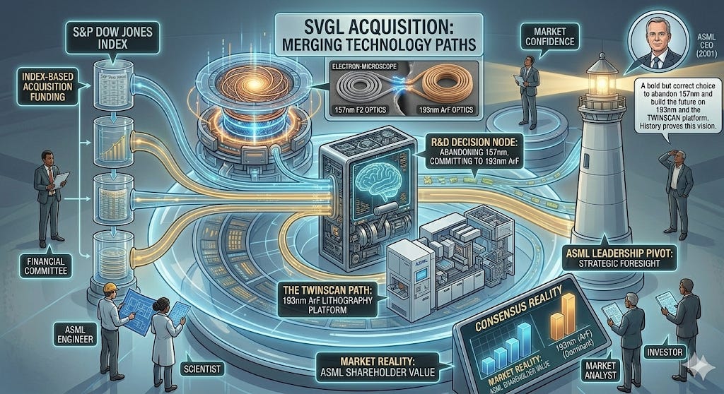
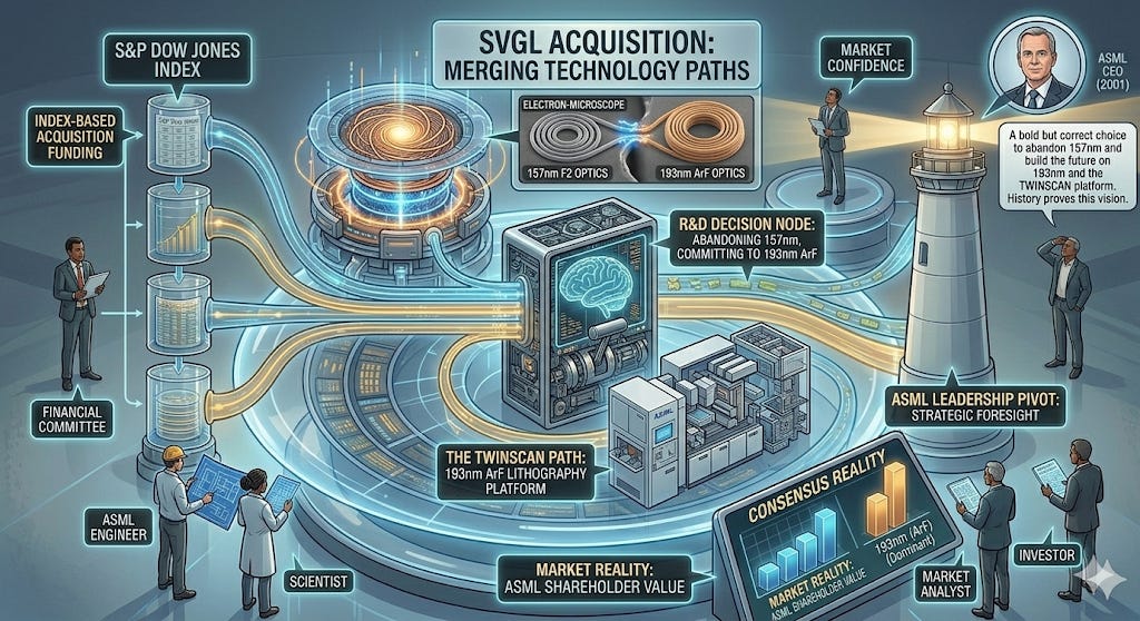
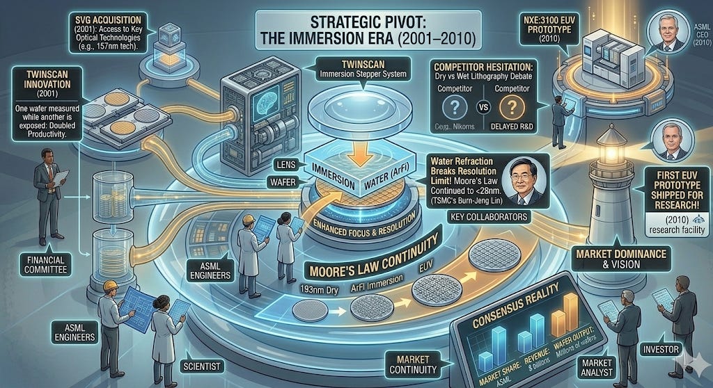
While competitors Nikon and Canon hesitated on new light sources, ASML made a strategic pivot to “Immersion Lithography,” putting a layer of water between the lens and the wafer to sharpen the focus.
2001: Launch of the TWINSCAN system. It allows one wafer to be measured while another is exposed, doubling productivity.
2001: Acquisition of Silicon Valley Group (SVG). This gives ASML a massive footprint in the US and access to key optical technologies.
2003: The Immersion Pivot. While the industry debated “Dry” vs “Wet” lithography, ASML (with TSMC’s Burn-Jeng Lin) moved aggressively into Immersion.
2004: Delivery of the first Immersion (ArFi) prototype. This effectively “broke” the resolution limits of the time and allowed Moore’s Law to continue to 28nm and below.
2010: ASML ships the first EUV prototype (NXE:3100) to a customer for research.
💎 Phase 4: The EUV Monopoly (2011–2020)
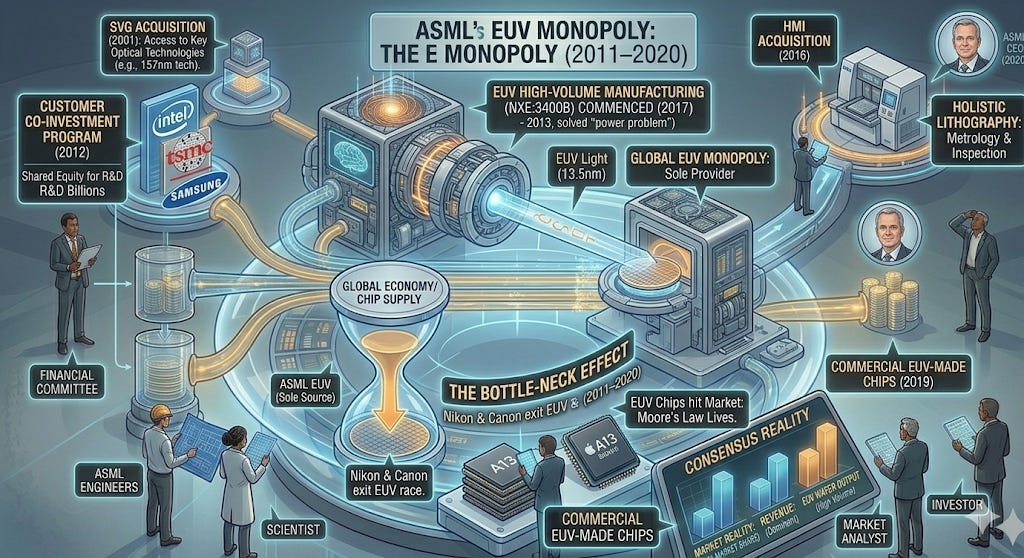
This decade cemented ASML as a “bottleneck” for the entire global economy. EUV was so difficult and expensive that Nikon and Canon officially dropped out of the race.
2012: The Customer Co-Investment Program. In a masterstroke of de-risking, ASML convinces its biggest customers—Intel, TSMC, and Samsung—to invest billions into ASML’s R&D in exchange for equity.
2013: Acquisition of Cymer, the San Diego-based light source manufacturer. This was vital to solving the “power problem” of EUV light.
2016: Acquisition of Hermes Microvision (HMI) for $3.1 billion to bolster “holistic” lithography (metrology and inspection).
2017: The first commercial EUV systems (NXE:3400B) begin shipping for high-volume manufacturing (HVM).
2019: The first EUV-made chips (iPhone 11) hit the market. ASML is now the sole provider of EUV machines globally.
⚡ Phase 5: High-NA & The AI Era (2021–Present)
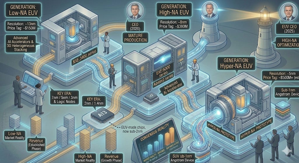
As 3nm and 2nm nodes approach, ASML is moving to “High-NA” (Numerical Aperture), which uses even larger optics to achieve higher resolution.
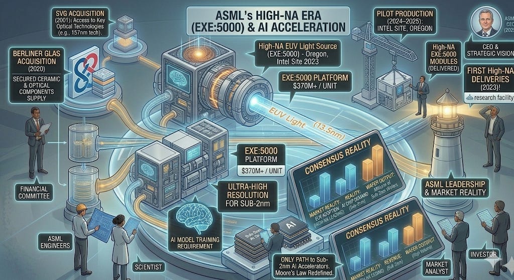
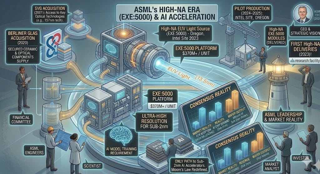
2020: Acquisition of Berliner Glas to secure the supply chain for ceramic and optical components.
2023: Delivery of the first High-NA EUV modules (the EXE:5000 platform) to Intel’s site in Oregon.
2024–2025: High-NA systems (costing ~$370M+ each) begin pilot production. These machines are the only way to produce the sub-2nm chips required for the next generation of AI accelerators.
To understand ASML’s position in 2026, you have to view it not just as a company, but as a geopolitical bottleneck. While most industries have competition, the high-end lithography market is a total monopoly.
Here is a breakdown of ASML’s technological moat and where the “fallen giants,” Nikon and Canon, stand today.
🏰 The Moat: Three Layers of Impossibility
ASML’s moat isn’t just a patent; it’s a combination of physics, supply chain control, and sheer capital intensity that no other company can match.
1. The Physics: Extreme Ultraviolet (EUV)
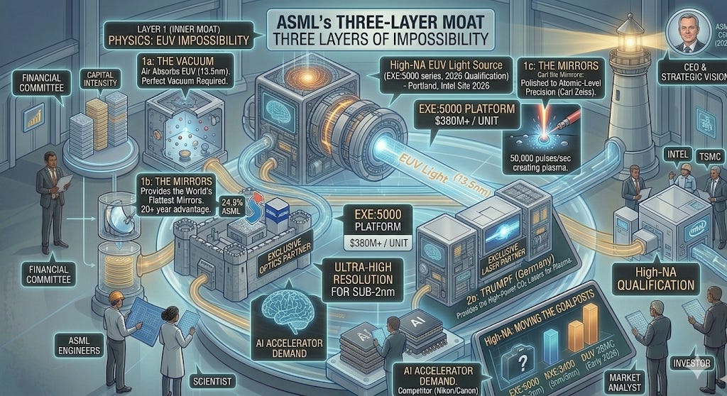
EUV light is notoriously difficult to work with. It has a wavelength of 13.5 nanometers—so small that it is absorbed by almost everything, including air.
The Vacuum: Because air absorbs EUV light, the entire machine must operate in a near-perfect vacuum.
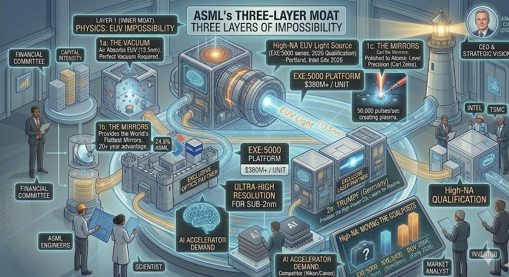
The Mirrors: You cannot use glass lenses for EUV. Instead, ASML uses the world’s flattest mirrors, polished to atomic-level precision by Carl Zeiss. If these mirrors were the size of Germany, the largest bump on them would be less than a millimeter high.
The Tin Droplets: To create EUV light, a laser blasts a microscopic droplet of molten tin twice—50,000 times per second. This creates a plasma that emits the light.
2. The Supplier Lockdown
ASML doesn’t build every part; they are the system integrator. They have locked down the world’s most advanced specialists into exclusive partnerships:
Carl Zeiss (Germany): Provides the mirrors. ASML owns a 24.9% stake in Zeiss SMT to ensure they remain the only customer for these optics.
Trumpf (Germany): Provides the high-power CO2 lasers required for the light source.
There is no “Plan B” for these suppliers. If you wanted to compete with ASML, you would first have to spend 20 years building a company that can rival Zeiss.
3. High-NA: Moving the Goalposts
Just as the world caught up to the idea of EUV, ASML launched High-NA (High Numerical Aperture).
These machines (the EXE:5000 series) cost upwards of $380 million each.
As of early 2026, Intel and TSMC are currently qualifying these for volume production. High-NA allows for even finer resolution (sub-2nm), effectively extending the “moat” for another decade.
🛠️ The Recurring Engine: Installed Base Management (IBM)
In the semiconductor world, buying an ASML machine is just the “entry fee.” The real relationship—and the most stable cash flow—comes from keeping those machines running 24/7 at 99% uptime.
1. The Financial Bedrock
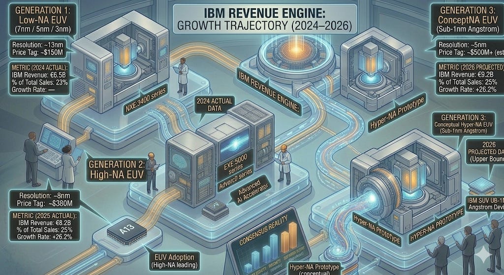
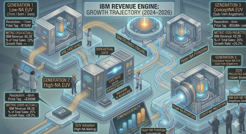
As of the full-year 2025 results, ASML’s service and field option sales (IBM) reached €8.2 billion, a staggering 26% increase over 2024.
Revenue Share: IBM now accounts for roughly 25% of total net sales.
Growth Trajectory: In 2025, while new system sales grew at a healthy clip, the service business grew more than twice as fast (26.2% vs 12.4% for systems).
High-Margin Nature: Service revenue typically carries higher and more stable gross margins than the initial hardware sale. As the fleet of EUV machines grows, this “software-like” recurring revenue stream expands automatically.
2. The “Field Option” Upsell
ASML doesn’t just fix broken parts; they sell performance upgrades for machines already on the factory floor.
Productivity Boosts: A customer can pay ASML millions to upgrade a 5-year-old DUV machine’s software or sensors, increasing its “wafer-per-hour” (wph) throughput by 10-15%.
CAPEX Efficiency: For a company like TSMC, it is often cheaper to pay ASML for a “Field Option” upgrade than to build a new cleanroom for a new machine. This makes ASML’s revenue “sticky” even when customers aren’t building new factories.
3. The EUV Service Multiplier
EUV machines are significantly more complex to maintain than older DUV systems.
The Complexity Premium: An EUV system has over 100,000 parts and miles of cabling. The service contracts for these machines are priced at a premium because they require specialized ASML engineers to be stationed permanently at the customer’s site.
Consumables: Components like the collector mirrors and tin-droplet generators require regular replacement and calibration, creating a literal “razor and blade” model for the most expensive machines in the world.
🇯🇵 The Competition: Where are Nikon and Canon?
Nikon and Canon were the kings of the 80s and 90s. Today, they have largely abandoned the “bleeding edge” to focus on different strategies.
📸 Nikon: The “Deep” Specialist
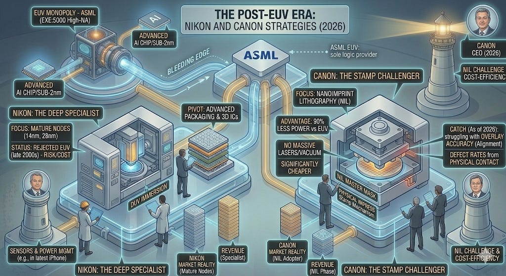
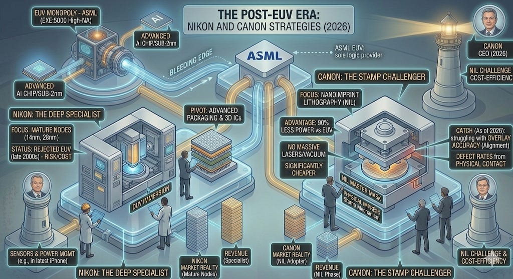
Nikon essentially lost the EUV race in the late 2000s when they decided the technology was too risky and expensive.
Current Status: They remain a strong player in DUV (Deep Ultraviolet) lithography.
The Strategy: They focus on “immersion” lithography for mature nodes (14nm, 28nm) and have pivoted heavily into Advanced Packaging and 3D ICs. While they don’t make the chips for the latest iPhone, they make the machines for many of the sensors and power management chips inside it.
🖨️ Canon: The “Stamp” Challenger
Canon has taken a completely different path. Instead of using light to “print” circuits, they are betting on Nanoimprint Lithography (NIL).
The Technology: Think of NIL as a high-tech “ink stamp.” It physically presses a master mask into the silicon wafer.
The Advantage: It is significantly cheaper and uses 90% less power than EUV because it doesn’t require massive lasers or vacuums.
The Catch: As of 2026, NIL still struggles with “overlay accuracy” (aligning multiple layers) and defect rates caused by the physical contact. It is currently used for simple, repetitive structures like NAND flash memory rather than the complex logic processors found in AI chips.
🏗️ The R&D Engine: Spending for the Next Decade
ASML doesn’t just iterate; they reinvent physics. Their R&D strategy is built on a “rolling roadmap” where they begin developing the next generation of machines before the current one has even shipped its first unit.
💰 The Numbers (2025–2026)
Annual R&D Spend: In 2025, ASML spent a record €4.7 billion on R&D—roughly 14% of their total revenue.
The AI Multiplier: ASML recently took a €1.3 billion stake in Mistral AI (roughly 11% ownership). They aren’t just making chips for AI; they are using AI to design the next generation of lithography software and diagnostics, effectively embedding AI into the “brain” of the machine to increase wafer yield.
The Talent Moat: They now employ over 44,000 people, with a massive percentage dedicated solely to “future-tech” engineering.
🔄 The Investment Cycle
ASML uses a Customer Co-Investment model that is unique in finance. By getting companies like Intel and TSMC to help fund the R&D for High-NA and beyond, ASML ensures:
Guaranteed Buyers: If you’ve invested billions in the R&D, you aren’t going to buy from a competitor.
De-risked Balance Sheet: They use their customers’ capital to build the very tools those customers will eventually pay $400M+ for.
🚀 The Next Frontier: “Hyper-NA” EUV
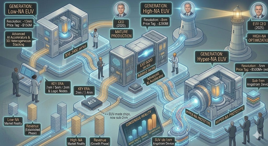
While the world is currently obsessing over High-NA (0.55 NA), ASML is already deep into the development of Hyper-NA (0.75 NA). This is the technology that will carry Moore’s Law into the 2030s.
What is Hyper-NA?
If High-NA is a better pair of glasses, Hyper-NA is a microscope. By increasing the Numerical Aperture to 0.75, ASML aims to print features as small as 5nm in a single exposure.
The Timeline: ASML and their optics partner, Carl Zeiss, are already in the design phase. They expect the first prototypes to appear around 2030.
The Power Problem: To make Hyper-NA work, ASML is developing a 1,000-watt to 1,500-watt light source (a 50%+ increase over current EUV). This requires firing 100,000 tin droplets per second—double the current rate.
The Goal: Mass production of sub-1nm (Angstrom-era) chips.
📉 Why this Kills Competition
The cost of developing Hyper-NA is estimated to be so high that even the combined efforts of Japan or China would struggle to fund the R&D alone. ASML is effectively “pricing out” the rest of the planet.
👨💼 The Leader: Christophe Fouquet
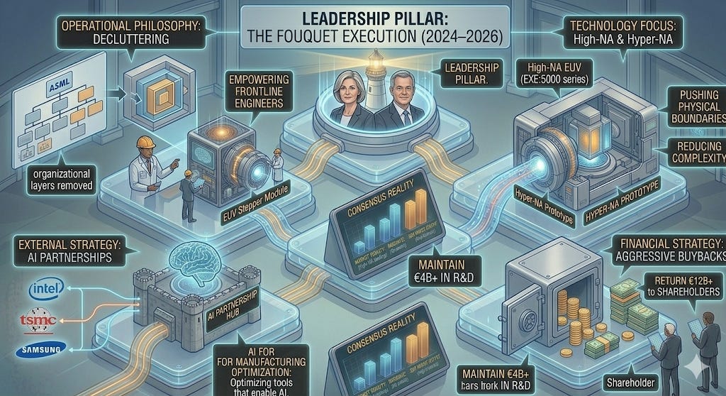
Fouquet is not an outsider; he is a 15-year ASML veteran who previously ran the EUV division. His strategy is defined by the phrase: “The faster you grow, the less efficient you get.” He is currently “rewiring” the company to ensure ASML doesn’t collapse under its own weight.
Vision: “Cost with a capital C”
Fouquet’s vision isn’t just about making better machines; it’s about the economic viability of Moore’s Law. The Thesis: He believes ASML’s primary job is to drive down the “Cost per Transistor.” If the machines (like High-NA) become too expensive for customers to make a profit, the industry stops.
Litho Intensity: He is betting on “Litho Intensity”—the idea that as chips get more complex, a larger percentage of a fab’s budget must go to ASML tools versus other equipment.
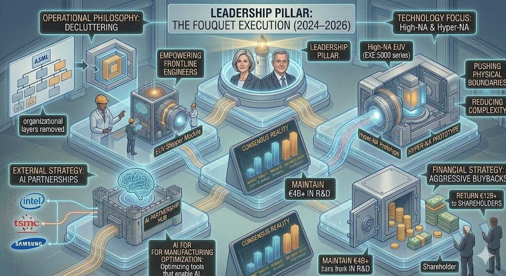
Strategy: The “Agility Overhaul” (January 2026)
In a bold move announced in early 2026, Fouquet initiated a massive internal restructuring. This is a classic “middle-manager” purge designed to return the company to its engineering roots.
Streamlining: He is cutting roughly 1,700 positions (mostly in Technology and IT) to remove “red tape.”
Product-Centric Teams: He is moving ASML away from a complex matrix structure to a setup where engineers are dedicated to specific product modules. The goal: Faster time-to-market.
AI Integration: Fouquet signed a landmark partnership with Mistral AI in late 2025. He isn’t just selling chips to AI companies; he is using Mistral’s LLMs to help ASML engineers navigate millions of lines of code and technical documentation more efficiently.
Execution: Customer Co-Dependence
Fouquet’s execution style is deeply collaborative. He has doubled down on the “Customer Team Model,” where ASML engineers essentially live at TSMC and Intel sites.
2026 Guidance: He has guided for €34B–€39B in sales for 2026, a massive jump from 2024 levels, driven by the “Big Ramp” of High-NA systems.
Capital Return: To keep investors happy during this transition, he recently authorized a €12 billion share buyback program (to be completed by 2028), signaling total confidence in the company’s cash-generating power.
💰 The Financial Engine: Monetizing a Monopoly